Home / Products / Components / SiC MOSFET
| Place of Origin: | Shanghai |
| Brand Name: | Inventchip Technology |
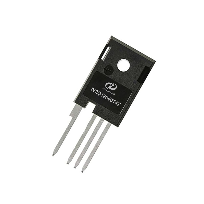
| Model Number: | IV2Q12040T4Z |
| Certification: | AEC-Q101 |
Features
2ndGeneration SiC MOSFET Technology with
+15~+18V gate drive
High blocking voltage with low on-resistance
High speed switching with low capacitance
175°C operating junction temperature capability
Ultra fast and robust intrinsic body diode
Kelvin gate input easing driver circuit design
AEC-Q101 qualified
Applications
EV chargers and OBCs
Solar boosters
Automotive compressor inverters
AC/DC power supplies
Outline:

Marking Diagram:

Absolute Maximum Ratings(TC=25°C unless otherwise specified)
| Symbol | Parameter | Value | Unit | Test Conditions | Note |
| VDS | Drain-Source voltage | 1200 | V | VGS =0V, ID =100μA | |
| VGSmax (Transient) | Maximum transient voltage | -10 to 23 | V | Duty cycle<1%, and pulse width<200ns | |
| VGSon | Recommended turn-on voltage | 15 to 18 | V | ||
| VGSoff | Recommended turn-off voltage | -5 to -2 | V | Typical -3.5V | |
| ID | Drain current (continuous) | 65 | A | VGS =18V, TC =25°C | Fig. 23 |
| 48 | A | VGS =18V, TC =100°C | |||
| IDM | Drain current (pulsed) | 162 | A | Pulse width limited by SOA and dynamic Rθ(J-C) | Fig. 25, 26 |
| ISM | Body diode current (pulsed) | 162 | A | Pulse width limited by SOA and dynamic Rθ(J-C) | Fig. 25, 26 |
| PTOT | Total power dissipation | 375 | W | TC =25°C | Fig. 24 |
| Tstg | Storage temperature range | -55 to 175 | °C | ||
| TJ | Operating junctiontemperature | -55 to 175 | °C | ||
| TL | Solder Temperature | 260 | °C | wave soldering only allowed at leads, 1.6mm from case for 10 s |
Thermal Data
| Symbol | Parameter | Value | Unit | Note |
| Rθ(J-C) | Thermal Resistance from Junction to Case | 0.4 | °C/W | Fig. 25 |
Electrical Characteristics (TC =25。C unless otherwise specified)
| Symbol | Parameter | Value | Unit | Test Conditions | Note | ||
| Min. | Typ. | Max. | |||||
| IDSS | Zero gate voltage drain current | 5 | 100 | μA | VDS =1200V, VGS =0V | ||
| IGSS | Gate leakage current | ±100 | nA | VDS =0V, VGS = -5~20V | |||
| VTH | Gate threshold voltage | 1.8 | 2.8 | 4.5 | V | VGS =VDS , ID =9mA | Fig. 8, 9 |
| 2.1 | VGS =VDS , ID =9mA @ TJ =175。C | ||||||
| RON | Static drain-source on - resistance | 40 | 52 | mΩ | VGS =18V, ID =20A @TJ =25。C | Fig. 4, 5, 6, 7 | |
| 75 | mΩ | VGS =18V, ID =20A @TJ =175。C | |||||
| 50 | 65 | mΩ | VGS =15V, ID =20A @TJ =25。C | ||||
| 80 | mΩ | VGS =15V, ID =20A @TJ =175。C | |||||
| Ciss | Input capacitance | 2160 | pF | VDS=800V, VGS =0V, f=1MHz, VAC=25mV | Fig. 16 | ||
| Coss | Output capacitance | 100 | pF | ||||
| Crss | Reverse transfer capacitance | 5.8 | pF | ||||
| Eoss | Coss stored energy | 40 | μJ | Fig. 17 | |||
| Qg | Total gate charge | 110 | nC | VDS =800V, ID =30A, VGS =-3 to 18V | Fig. 18 | ||
| Qgs | Gate-source charge | 25 | nC | ||||
| Qgd | Gate-drain charge | 59 | nC | ||||
| Rg | Gate input resistance | 2.1 | Ω | f=1MHz | |||
| EON | Turn-on switching energy | 446.3 | μJ | VDS =800V, ID =30A, VGS =-3.5 to 18V, RG(ext) =3.3Ω, L=200μH TJ =25。C | Fig. 19, 20 | ||
| EOFF | Turn-off switching energy | 70.0 | μJ | ||||
| td(on) | Turn-on delay time | 9.6 | ns | ||||
| tr | Rise time | 22.1 | |||||
| td(off) | Turn-off delay time | 19.3 | |||||
| tf | Fall time | 10.5 | |||||
| EON | Turn-on switching energy | 644.4 | μJ | VDS =800V, ID =30A, VGS =-3.5 to 18V, RG(ext) =3.3Ω,L=200μH TJ =175。C | Fig. 22 | ||
| EOFF | Turn-off switching energy | 73.8 | μJ | ||||
Reverse Diode Characteristics (TC =25。C unless otherwise specified)
| Symbol | Parameter | Value | Unit | Test Conditions | Note | ||
| Min. | Typ. | Max. | |||||
| VSD | Diode forward voltage | 4.2 | V | ISD =20A, VGS =0V | Fig. 10, 11, 12 | ||
| 4.0 | V | ISD =20A, VGS =0V, TJ =175。C | |||||
| IS | Diode forward current (continuous) | 63 | A | VGS =-2V, TC =25。C | |||
| 36 | A | VGS =-2V, TC=100。C | |||||
| trr | Reverse recovery time | 42.0 | ns | VGS=-3.5V/+18V, ISD =30A, VR =800V, RG(ext) =10Ω L=200μH di/dt=3000A/μs | |||
| Qrr | Reverse recovery charge | 198.1 | nC | ||||
| IRRM | Peak reverse recovery current | 17.4 | A | ||||
Typical Performance (curves)


Package Dimensions


Note:
1. Package Reference: JEDEC TO247, Variation AD
2. All Dimensions are in mm
3. Slot Required, Notch May Be Rounded
4. Dimension D&E Do Not Include Mold Flash
5. Subject to Change Without Notice
 EN
EN
 AR
AR
 HR
HR
 DA
DA
 NL
NL
 FR
FR
 DE
DE
 EL
EL
 HI
HI
 IT
IT
 JA
JA
 KO
KO
 NO
NO
 PL
PL
 PT
PT
 RO
RO
 RU
RU
 ES
ES
 SV
SV
 TL
TL
 IW
IW
 ID
ID
 LT
LT
 SR
SR
 SK
SK
 UK
UK
 VI
VI
 SQ
SQ
 HU
HU
 TH
TH
 TR
TR
 FA
FA
 AF
AF
 MS
MS
 HY
HY
 BN
BN
 LA
LA
 TA
TA
 TE
TE
 MY
MY