| Miesto pôvodu: | Zhejiang |
| Názov značky: | Inventchip Technology |
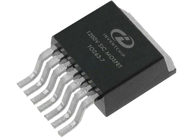
| Číslo modelu: | IV1B12013HA1L |
| Certifikácia: | AEC-Q101 |
Vlastnosti
Vysoké blokovacie napätie s nízkym odporom pri vedení
Rýchle preklápajúce sa s nízkou kapacitou
Vysoká schopnosť prevádzky pri spojovacej teplote
Veľmi rýchla a robustná vlastná vnútorná dióda
Použitie
Solárne aplikácie
Systém neprerušiteľného zdroja energie (UPS)
Motorové ovládače
Vysokonapätové konvertory DC/DC
Balík

Označovací diagram

Absolútne maximálne hodnoty (TC=25°C pokiaľ nie je uvedené inak)
| Súbor | Parametre | Hodnota | Jednotka | Podmienky testovania | Poznámka |
| VDS | Napätie medzi odberárom a zdrojom | 1200 | V | ||
| VGSmax (DC) | Maximálne DC napätie | -5 do 22 | V | Statické (DC) | |
| VGSmax (Výpěnka) | Maximálna bodová napätie | -10 do 25 | V | <1% časová zložka, a šírka impulzu <200ns | |
| VGSon | Odporúčané napätie zapnutia | 20±0.5 | V | ||
| VGSoff | Odporúčané napätie vypnutia | -3.5 do -2 | V | ||
| ID | Prúd drainu (neustály) | 96 | A | VGS =20V, Th =50°C, Tvj≤150℃ | |
| 102 | A | VGS =20V, Th =50°C, Tvj≤175℃ | |||
| IDM | Prúd drainu (impulzívny) | 204 | A | Šírka impulzu obmedzená SOA | Obr.26 |
| PTOT | Celkové spotrebované výkon | 210 | V | Tvj≤150℃ | Obr.24 |
| Tstg | Rozsah teploty skladovania | -40 do 150 | °C | ||
| TJ | Maximálna virtuálna teplota spojov pri prechodových podmienkach | -40 do 150 | °C | Operácia | |
| -55 do 175 | °C | Intermitentne s redukovanej životnosťou |
Teplotné údaje
| Súbor | Parametre | Hodnota | Jednotka | Poznámka |
| Rθ(J-H) | Termická odpornosť od spojenia ku chladnici | 0.596 | °C/W | Obr.25 |
Elektrické charakteristiky (TC=25°C pokiaľ nie je uvedené inak)
| Súbor | Parametre | Hodnota | Jednotka | Podmienky testovania | Poznámka | ||
| Min. | Typ. | Max, čo sa deje? | |||||
| IDSS | Drenážny prúd pri nulovej gatovej napäťe | 10 | 200 | μA | VDS =1200V, VGS =0V | ||
| IGSS | Utečový prúd brány | ±200 | nA | VDS =0V, VGS = -5~20V | |||
| VTH | Prahové napätie brány | 1.8 | 3.2 | 5 | V | VGS=VDS , ID =24mA | Obr.9 |
| 2.3 | VGS=VDS , ID =24mA @ TC =150. C | ||||||
| Železo | Statický odpor medzi drainom a zdrojom v stave zapnutia | 12.5 | 16.3 | mΩ | VGS =20V, ID =80A @TJ =25. C | Obr.4-7 | |
| 18 | mΩ | VGS =20V, ID =80A @TJ =150. C | |||||
| Ciss | Vstupná kapacita | 11 | nF | VDS=800V, VGS =0V, f=100kHZ , VAC =25mV | Obr.16 | ||
| Coss | Výstupná kapacita | 507 | pF | ||||
| Crss | Kapacita opačného prenosu | 31 | pF | ||||
| Eoss | Uložená energia Coss | 203 | μJ | Obr.17 | |||
| Qg | Celkový vratný náboj | 480 | nC | VDS = 800V, ID = 80A, VGS = -5 až 20V | Obr. 18 | ||
| Qgs | Náboj medzi bránou a zdrojom | 100 | nC | ||||
| Qgd | Náboj medzi bránou a drenom | 192 | nC | ||||
| Rg | Vstupný odpor brány | 1.0 | ω | f=100kHZ | |||
| EON | Energetické prepnutie pri zapnutí | 783 | μJ | VDS =600V, ID =60A, VGS=-5 až 20V, RG(ext)na/ RG(ext)vyp =2.5Ω/1.43Ω, L=120μH | Obraz.19-22 | ||
| EOFF | Energetické prepnutie pri vypnutí | 182 | μJ | ||||
| td(zač) | Čas oneskorenia pri zapnutí | 30 | nS | ||||
| tr | Čas nárastu | 5.9 | |||||
| td(vyp) | Čas oneskorenia pri vypnutí | 37 | |||||
| tF | Čas pádu | 21 | |||||
| LsCE | Nehodnotená indukcia | 7.6 | nH | ||||
Vlastnosti reverzného diódy (TC=25°C pokiaľ nie je uvedené inak)
| Súbor | Parametre | Hodnota | Jednotka | Podmienky testovania | Poznámka | ||
| Min. | Typ. | Max, čo sa deje? | |||||
| VSD | Predná diódová elektrická súčasť | 4.9 | V | ISD =80A, VGS =0V | Obr.10- 12 | ||
| 4.5 | V | ISD =80A, VGS =0V, TJ =150°C | |||||
| trr | Čas opačného obnovenia | 17.4 | nS | VGS =-5V/+20V, ISD =60A, VR =600V, di/dt=13.28A/ns, RG(ext) =2.5Ω, L=120μH | |||
Qrr |
Náboj opačného obnovenia | 1095 | nC | ||||
| IRRM | Maximálny vrcholný prúd opačného obnovenia | 114 | A | ||||
Charakteristiky NTC termistoru
| Súbor | Parametre | Hodnota | Jednotka | Podmienky testovania | Poznámka | ||
| Min. | Typ. | Max, čo sa deje? | |||||
| RNTC | Nominálny odpor | 5 | kΩ | TNTC =25℃ | Obr.27 | ||
| δR/R | Tolerancia odporu pri 25℃ | -5 | 5 | % | |||
| β25/50 | Beta hodnota | 3380 | K | ±1% | |||
| Pmax | Spotreba energie | 5 | mW | ||||
Typické vlastnosti (krivky)


Rozmery obalu (mm)

 EN
EN
 AR
AR
 HR
HR
 DA
DA
 NL
NL
 FR
FR
 DE
DE
 EL
EL
 HI
HI
 IT
IT
 JA
JA
 KO
KO
 NO
NO
 PL
PL
 PT
PT
 RO
RO
 RU
RU
 ES
ES
 SV
SV
 TL
TL
 IW
IW
 ID
ID
 LT
LT
 SR
SR
 SK
SK
 UK
UK
 VI
VI
 SQ
SQ
 HU
HU
 TH
TH
 TR
TR
 FA
FA
 AF
AF
 MS
MS
 HY
HY
 BN
BN
 LA
LA
 TA
TA
 TE
TE
 MY
MY